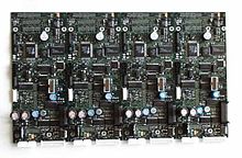
Depaneling

Depaneling or depanelization is a process step in high-volume electronics assembly production. In order to increase the throughput of printed circuit board (PCB) manufacturing and surface mount (SMT) lines, PCBs are often arranged in a process called panelization so that they consist of many smaller individual PCBs that will be used in the final product. This PCB cluster is called a panel or multiblock. The large panel is broken up or "depaneled" as a certain step in the process - depending on the product, it may happen right after SMT process, after in-circuit test (ICT), after soldering of through-hole elements, or even right before the final assembly of the PCB assembly (PCBA) into the enclosure.
Risks[edit]
When selecting a depaneling technique, it is important to be mindful of the risks, including:
- Mechanical strain: depaneling can be a violent operation and may bend the PCB causing some components to fracture, or in the worst case, break traces. Ways to mitigate this are avoiding placing components near the edge of the PCBA, and orienting components parallel to the break line.
- Tolerance: some methods of depaneling may result in the PCBA being a different size than intended. Ways to mitigate are to communicate with the manufacturer about which dimensions are critical, and selecting a depaneling method that meets your needs. Hand depaneling will have the loosest tolerance, laser depaneling the tightest.
Main depanel technologies[edit]
There are six main depaneling cutting techniques currently in use:
- hand break
- pizza cutter / V-cut
- punch
- router
- saw
- laser
Hand break[edit]
This method is suitable for strain-resistant circuits (e.g. without SMD components). The operator simply breaks the PCB, usually along a prepared V-groove line, with the help of a proper fixture.
Pizza cutter / V-cut[edit]
A pizza cutter is a rotary blade, sometimes rotating using its own motor. The operator moves a pre-scored PCB along a V-groove line, usually with the help of a special fixture. This method is often used only for cutting huge panels into smaller ones. The equipment is cheap and requires only sharpening of the blade and greasing as maintenance.
It uses an aluminium based jig to secure the PCB in place.
Punch[edit]
Punching is a process where single PCBs are punched out of the panel through the use of special fixture. It is a two-part fixture, with sharp blades on one part and supports on the other. The production capacity of such a system is high, but fixtures are quite expensive and require regular sharpening.
Router[edit]
A depaneling router is a machine similar to wood router. It uses a router bit to mill the material of the PCB. The hardness of the PCB material wears down the bit, which must be replaced periodically.
Routing requires that single boards are connected using tabs in a panel. The bit mills the whole material of the tab. It produces much dust that has to be vacuumed. It is important for the vacuum system to be ESD-safe. Also the fixturing of the PCB must be tight - usually an aluminium jig or a vacuum holding system is used.
The two most important parameters of the routing process are: feed rate and rotational speed. They are chosen according to the bit type and diameter and should remain proportional (i.e. increasing feed rate should be done together with increasing the rotational speed).
Routers generate vibrations of the same frequency as their rotational speed (and higher harmonics), which might be important if there are vibration-sensitive components on the surface of the board. The strain level is lower than for other depaneling methods. Their advantage is that they are able to cut arcs and turn at sharp angles. Their disadvantage is lower capacity.
Saw[edit]
A saw is able to cut through panels at high feed rates. It can cut both V-grooved and not-V-grooved PCBs. It does not cut much material and therefore generates low amounts of dust.
The disadvantages are: ability to cut in straight lines only and higher stress than for routing.
Laser[edit]
Laser cutting is now being offered as an additional method by some manufacturers.
UV laser depaneling makes use of a 355 nm wavelength (ultraviolet), diode-pumped, Nd:YAG laser source. At this wavelength the laser is capable of cutting, drilling and structuring on rigid and flex circuit substrates. The laser beam, capable of cut widths under 25 μm, is controlled by high-precision, galvo-scanning mirrors with repeat accuracy of +/-4 μm.[1]
A variety of substrate materials can be cut with a UV laser source including FR-4 and similar resin-based substrates, polyimide, ceramics, PTFE, PET, aluminium, brass and copper.
Advantages: accuracy, precision, low mechanical stress and flexible contour and cut capabilities.
Disadvantages: initial capital investment is often higher than traditional depaneling technologies, also the optimal board thickness is recommended to be no more than 1 mm.
CO2 laser sources have also been used for depaneling, but are considered outdated as UV laser technology provides cleaner cuts, less-thermal stress and higher precision capabilities.
See also[edit]
References[edit]
- ^ Meier, Dieter J.; Schmidt, Stephan H. (c. 2002). "PCB Laser Technology for Rigid and Flex HDI – Via Formation, Structuring, Routing" (PDF). Garbsen, Germany; Wilsonville, Oregon, USA: LPKF Laser & Electronics AG. Archived (PDF) from the original on 2024-02-24. Retrieved 2024-02-24. (5 pages)
