Vacuum deposition
This article includes a list of references, related reading, or external links, but its sources remain unclear because it lacks inline citations. (April 2009) |

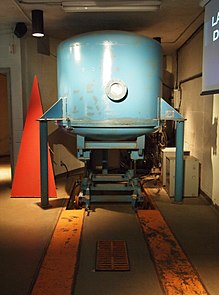
Vacuum deposition is a group of processes used to deposit layers of material atom-by-atom or molecule-by-molecule on a solid surface. These processes operate at pressures well below atmospheric pressure (i.e., vacuum). The deposited layers can range from a thickness of one atom up to millimeters, forming freestanding structures. Multiple layers of different materials can be used, for example to form optical coatings. The process can be qualified based on the vapor source; physical vapor deposition uses a liquid or solid source and chemical vapor deposition uses a chemical vapor.[2]
Description
[edit]The vacuum environment may serve one or more purposes:
- reducing the particle density so that the mean free path for collision is long
- reducing the particle density of undesirable atoms and molecules (contaminants)
- providing a low pressure plasma environment
- providing a means for controlling gas and vapor composition
- providing a means for mass flow control into the processing chamber.
Condensing particles can be generated in various ways:
- thermal evaporation
- sputtering
- cathodic arc vaporization
- laser ablation
- decomposition of a chemical vapor precursor, chemical vapor deposition
In reactive deposition, the depositing material reacts either with a component of the gaseous environment (Ti + N → TiN) or with a co-depositing species (Ti + C → TiC). A plasma environment aids in activating gaseous species (N2 → 2N) and in decomposition of chemical vapor precursors (SiH4 → Si + 4H). The plasma may also be used to provide ions for vaporization by sputtering or for bombardment of the substrate for sputter cleaning and for bombardment of the depositing material to densify the structure and tailor properties (ion plating).
Types
[edit]When the vapor source is a liquid or solid the process is called physical vapor deposition (PVD). When the source is a chemical vapor precursor, the process is called chemical vapor deposition (CVD). The latter has several variants: low-pressure chemical vapor deposition (LPCVD), plasma-enhanced chemical vapor deposition (PECVD), and plasma-assisted CVD (PACVD). Often a combination of PVD and CVD processes are used in the same or connected processing chambers.
Applications
[edit]- Electrical conduction: metallic films, resistors, transparent conductive oxides (TCOs), superconducting films & coatings
- Semiconductor devices: semiconductor films, electrically insulating films
- Solar cells
- Optical films: anti-reflective coatings, optical filters
- Reflective coatings: mirrors, hot mirrors
- Tribological coating: hard coatings, erosion resistant coatings, solid film lubricants
- Energy conservation & generation: low emissivity glass coatings, solar absorbing coatings, mirrors, solar thin film photovoltaic cells, smart films
- Magnetic films: magnetic recording
- Diffusion barrier: gas permeation barriers, vapor permeation barriers, solid state diffusion barriers
- Corrosion protection:
- Automotive applications: lamp reflectors and trim applications
- Vinyl record pressing, manufacture of gold and platinum records
A thickness of less than one micrometre is generally called a thin film, while a thickness greater than one micrometre is called a coating.
See also
[edit]- Ion plating
- Sputter deposition
- Cathodic arc deposition
- Spin coating
- Metallised film
- Molecular vapor deposition
References
[edit]- ^ "Daily events and images of the installation of the BBSO New Solar Telescope". Big Bear Solar Observatory. Retrieved 6 January 2020.
- ^ Quintino, Luisa (2014). "Overview of coating technologies". Surface Modification by Solid State Processing. pp. 1–24. doi:10.1533/9780857094698.1. ISBN 9780857094681.
Bibliography
[edit]- SVC, "51st Annual Technical Conference Proceedings" (2008) SVC Publications ISSN 0737-5921 (previous proceeding available on CD)
- Anders, Andre (editor) "Handbook of Plasma Immersion Ion Implantation and Deposition" (2000) Wiley-Interscience ISBN 0-471-24698-0
- Bach, Hans and Dieter Krause (editors) "Thin Films on Glass" (2003) Springer-Verlag ISBN 3-540-58597-4
- Bunshah, Roitan F (editor). "Handbook of Deposition Technologies for Films and Coatings", second edition (1994)
- Glaser, Hans Joachim "Large Area Glass Coating" (2000) Von Ardenne Anlagentechnik GmbH ISBN 3-00-004953-3
- Glocker and I. Shah (editors), "Handbook of Thin Film Process Technology", Vol.1&2 (2002) Institute of Physics ISBN 0-7503-0833-8 (2 vol. set)
- Mahan, John E. "Physical Vapor Deposition of Thin Films" (2000) John Wiley & Sons ISBN 0-471-33001-9
- Mattox, Donald M. "Handbook of Physical Vapor Deposition (PVD) Processing" 2nd edition (2010) Elsevier ISBN 978-0-8155-2037-5
- Mattox, Donald M. "The Foundations of Vacuum Coating Technology" (2003) Noyes Publications ISBN 0-8155-1495-6
- Mattox, Donald M. and Vivivenne Harwood Mattox (editors) "50 Years of Vacuum Coating Technology and the Growth of the Society of Vacuum Coaters" (2007), Society of Vacuum Coaters ISBN 978-1-878068-27-9
- Westwood, William D. "Sputter Deposition", AVS Education Committee Book Series, Vol. 2 (2003) AVS ISBN 0-7354-0105-5
- Willey, Ronald R. "Practical Monitoring and Control of Optical Thin Films (2007)" Willey Optical, Consultants ISBN 978-0-615-13760-5
- Willey, Ronald R. "Practical Equipment, Materials, and Processes for Optical Thin Films" (2007) Willey Optical, Consultants ISBN 978-0-615-14397-2
